Energy level alignment of Cu(In,Ga)(S,Se)2 absorber compounds with In2S3, NaIn5S8, and CuIn5S8 buffer materials
E. Ghorbani,
P. Erhart,
and
K. Albe
Physical Review Materials 3, 31489
(2019)
doi: 10.1103/PhysRevMaterials.3.075401
Download PDF
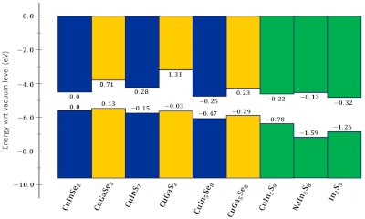
Motivated by environmental reasons, In2S3 is a promising candidate for a Cd-free buffer layer in Cu(In,Ga)(S,Se)2 (CIGSSe)-based thin film solar cells. For an impactful optimization of the In2S3 alternative buffer layer, however, a comprehensive knowledge of its electronic properties across the absorber-buffer interface is of foremost importance. In this respect, finding a favorable band offset between absorber and buffer layers can effectively reduce the carrier recombination at the interface and improve open circuit voltage and fill factor, leading to higher conversion efficiencies. In this study, we investigate the band alignment between the most common CIGSSe-based absorber compounds and In2S3. Furthermore, we consider two chemically modified indium sulfide layers, NaIn5S8 and CuIn5S8, and discuss how formation of these secondary phases influences band discontinuity across the interface. Our analysis is based on density functional theory calculations using hybrid functionals. The results suggest that Ga-based absorbers form a destructive cliff-like conduction band offset (CBO) with both pure and chemically modified buffer systems. For In-based absorbers, however, if the absorber layer is Cu-poor at the surface, a modest favorable spike-like CBO arises with NaIn5S8 and CuIn5S8.